
|
We are interested in:
|
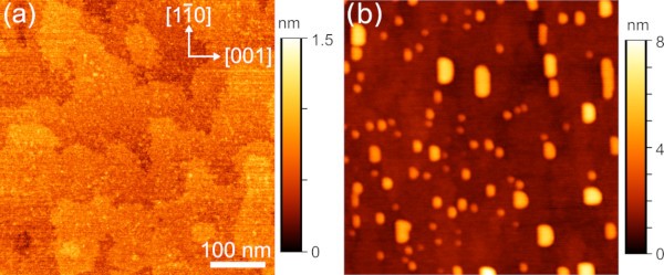
Atomic force topographs of a 2 monlayer thick InAs film on GaAs(110) before (a) and after (b) exposure to a Bi surfactant flux. The surfactant provokes the on-demand formation of InAs quantum dots.
|
|
Semiconductor nanostructures offer many advantages over conventional device structures based on planar heterostructures (planar layers grown on a bulk substrate). For example, while planar heterostructures are generally restricted to material combinations with similar lattice constants, the small size and mechanical flexibility of nanostructures allows for highly lattice-mismatched heterostructures to be realized, presenting the opportunity to fabricate heterostructures with previously prohibited materials combinations and strain states. This opens the door to a wide range of device applications and presents a promising route for integrating III-V materials (the basis for optoelectronic devices) on silicon (the basis for microelectronics and Si photonics), leading to on-chip optical data communication as part of next-generation telecommunications technologies.
|
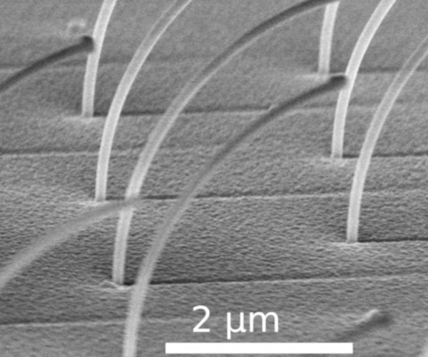
SEM image of a bent nanowire heterostructure
|
|
A primary focus of our research is the self-assembly of nanostructures by molecular beam epitaxy (MBE) and metalorganic chemical vapor deposition (MOCVD). These are the primary deposition techniques used in research and industry to fabricate ultrapure single-crystal semiconductor layers, especially for optoelectronic devices. We seek to understand and then engineer surface, strain and size/quantum effects which are inherent to nanostructures, in order to realize novel heterostructures and devices with new properties and functionalities.”
|
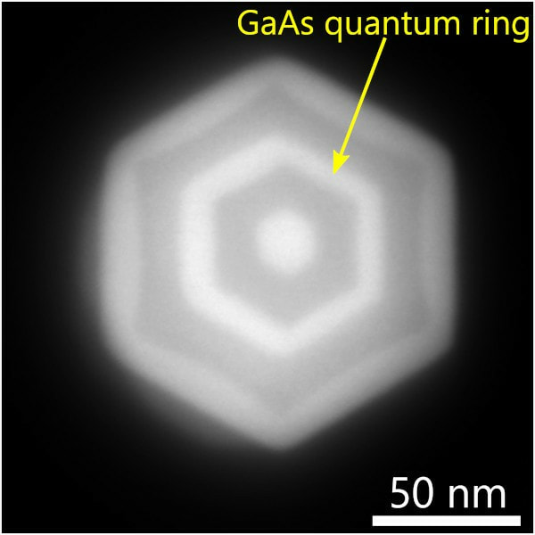
GaAs quantum ring within a GaAs/AlAs core-shell nanowire
|
Current Opportunities
Bent nanowire biosensors and optical interconnects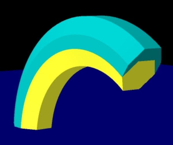
Illustration of a bent nanowire. Bending results from strain sharing between the core and an asymmetric shell.
We aim to develop a new bottom-up self-assembly approach to nanowire device fabrication by engineering the strain state and geometry of nanowire heterostructures.
U-shaped nanowire biosensors [e.g., chemical field-effect-transistors (FETs) and novel strain-based sensors], and optical interconnects for photonics applications will be explored. Applications
|
Surfactant-directed quantum-dot self-assembly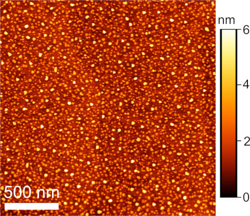
Surfactant-induced 3D islands on GaAs(111)A: potential entangled photon emitters.
This project will investigate using surface-energy-modifying "surfactants" (Bi/Sb) to externally induce the formation of strained quantum dots on substrates where their formation was not previously possible.
The goal is to realize optically-active (In,Ga)As quantum dots on non-(001) surfaces, and to develop novel single/entangled photon sources for quantum optics applications based on these structures. Applications
|
Postdoctoral fellow position in III-V epitaxy (MOCVD/MOVPE)
Prof. Ryan Lewis’ research group in the Department of Engineering Physics at McMaster University is seeking to hire a postdoctoral fellow (PDF) to investigate the metalorganic chemical vapor deposition (MOCVD) of III-V materials and nanostructures for optoelectronic applications.
The PDF will be responsible for the operation of a Structured Materials Industries (SMI) MOCVD/MOVPE reactor (installed in 2016). Current III-V growth activities being pursued in Dr. Lewis’ research lab include surfactant-enhanced (Sb/Bi) growth of quantum dots, orientation-patterned III-V structures for nonlinear lasers, strain engineering in III-V nanowires and surfactant-enhanced III-V growth on Si. The PDF will be expected to carry out MOCVD research relating to one or more of these topics, and will collaborate with and support PhD students working with the MOCVD.
More information can be found in the attached file below:
| mcmaster_mocvd_pdf_2022.pdf |